legacy home


non-o/s home
 
classic notches
 
24k, 68.15k...
 
without 24k
 
lpf with peak


This schematic assumes a buffer at its output (scroll down, please), and hence the coupling cap is included. (However, I couldn't include a buffer in the simulation with a wave file as a current source. Simulation with wav file threats wav file only as a full level signal, which for the current source means 1A.)


Appropriate squarewave.


The filter with the buffer included. Capacitor C4 can be omitted if output DC offset is sufficiently low. This stuff is not built and measured, but while we are at the topic... JFETs take a series series resistor at the input for best performance, and other than that, this is the complete non-o/s DAC's output stage with treble roll-off compensation, 3rd order low pass filter and very good driving capabilities.


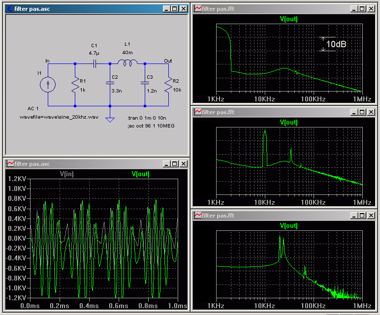
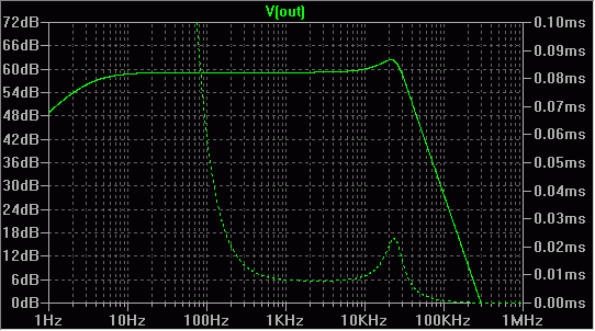
Now, one graph which includes frequency domain aspect of the filter, but with the group delay instead of the phase. Seen this way, it is possible to understand the use of the bigger coupling caps. While at 20 Hz the amplitude roll-off is 0.1dB (even if speakers and room could reproduce it, it is inaudible), and while looking at the phase error situation is still not bad at all, things, however, are not so good if group delay is considered. This may be important, but again, this is only one side of the thing. Get back to the topic - this graph is about the peak in the group delay in the treble. It is directly related to the 
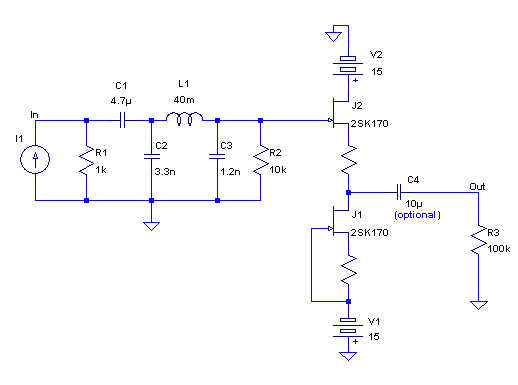
peak in the amplitude. Actually, since the FET does not affect this anyway, graph also shows the response of the circuit shown at the top of this page.